
Result Tap into unprecedented performance scalability and security for every workload with the NVIDIA H100 Tensor Core GPU. Result GTC NVIDIA today announced that the NVIDIA H100 Tensor Core GPU is in full production with global tech partners planning in October to. Result The card will be available in the next several months and it looks like it will be considerably more expensive than Nvidias current generation. Built on a custom TSMC 4N process Nvidia Today at its GPU Technology Conference GTC. Result Today during the 2022 NVIDIA GTC Keynote address NVIDIA CEO Jensen Huang introduced the new NVIDIA H100 Tensor Core GPU based on the..
Hpcwire
An Order-of-Magnitude Leap for Accelerated Computing. FREE delivery March 14 - 20 Or fastest delivery Tomorrow March 8. Web The H100 is NVIDIAs first GPU to support PCIe Gen5 providing the highest speeds possible at 128GBs bi. Web Nvidias H100 PCIe 50 compute accelerator carries the companys latest GH100 compute GPU. Web The NVIDIA H100 PCIe operates unconstrained up to its maximum thermal design power TDP level of 350 W to. NVIDIA H100 80GB HBM2e PCIE Express GPU Graphics Card New..
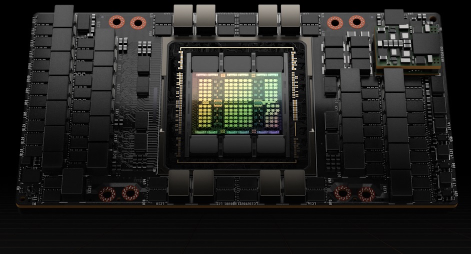
WEB For LLMs up to 175 billion parameters the PCIe-based H100 NVL with NVLink bridge utilizes Transformer Engine NVLink and 188GB HBM3 memory to provide optimum performance and. WEB The NVIDIA H100 card is a dual-slot 105 inch PCI Express Gen5 card based on the NVIDIA Hopper architecture It uses a passive heat sink for cooling which requires system airflow to operate the. WEB The NVIDIA H100 NVL card is a dual-slot 105 inch PCI Express Gen5 card based on the NVIDIA Hopper architecture It uses a passive heat sink for cooling which requires system airflow to. WEB This datasheet details the performance and product specifications of the NVIDIA H100 Tensor Core GPU It also explains the technological breakthroughs of the NVIDIA Hopper architecture. WEB Nvidias H100 PCIe 50 compute accelerator carries the companys latest GH100 compute GPU with 729614592 FP64FP32 cores see exact specifications below that..

Techpowerup
NVIDIA H100 PCIe cards use three NVIDIA NVLink bridges They are the same as the bridges used with NVIDIA A100 PCIe cards. For LLMs up to 175 billion parameters the PCIe-based H100 NVL with NVLink bridge utilizes Transformer Engine NVLink and 188GB HBM3 memory to. NVIDIA NVLink is a high-speed point-to-point P2P peer transfer connection Where one GPU can transfer data to and receive data from one other GPU. A single NVIDIA H100 Tensor Core GPU supports up to 18 NVLink connections for a total bandwidth of 900 gigabytes per second GBsover 7X the bandwidth. Fourth-generation NVLink and PCIe Gen 5 The NVIDIA H100 GPU with a PCIe Gen 5 board form-factor includes the following units..


Comments